MFD reverse engineering
 Roeurn Tourn
 This portion took a number of days and in some ways is ongoing. The MFDs are separated into two sub-systems: CRT display, and button & LED IO. Each system is logically separated and do not interact between each other. I’m only concerned with the Button IO.
Button board subsystem
The button IO subsystem contains a board called a Button Board, with 8 connectors for the LED buttons on top, and a DB-16 connector on the bottom. A jumper on left is used to distinguish between different button boards on the same ribbon cable. There are 7 solid state logic ICs on the board. They are listed below in order of logical significance. ;)
U1: 74HCT164 8 bit serial-in parallel out shift register
U2: GD54HC00 quad 2 input NAND gate
(used with the jumpers as part of board selection process)
U3: 5821 8 bit serial in Latched Drivers
U5: 5821 8 bit serial in Latched Drivers
(used to output to the LEDs)
U6: CD74HC165 8 bit parallel-in Serial out Shift register.
U7: CD74HC165 8 bit parallel-in Serial out Shift register.
U4: HD7405P HEX inverter
(used as part of the button input, and outputting circuit to the RIO board)
Wishing for x-rays
The intermediate goal is to draw a schematic of the button board. Simply looking at the traces is hampered by the plastic bits of the sockets and headers. I would like to x-ray of the board and redraw the schematic from the traces. (To overcome this problem in the future I think I want to build an x-ray machine at some point. )Having a schematic would allow me to figure out the cable used to communicate over the cable.
For now I only need to know what pins are the input pins and what pins are output pins so I could begin drafting the circuit board to control this device. Because the system uses solid state logic it is possible to determine uses and protocols by the arrangement and presence of the ICs on the board. Each chip has an designated input pin and an output pin.
Starbucks mochas and odd looks
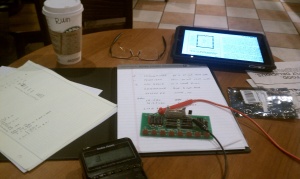 To find these pins, I took the board, my multimeter and went to Starbucks. A vanilla mocha and some time doing continuity testing, allowed me to determine that most of the lines on the db-16 line were power and ground, one line was attached to all the CLK inputs on all the ICs, and input 3 data lines, with 1 data output line .
Knowing witch is input and output is all I need to begin building a replacement board to interface the MFDs. More on that in the next post. And yes, they did misspell my name:)

Reader Comments